


The content below is taken from the original ( The Bus That’s Not A Bus: The Joys Of Hacking PCI Express), to continue reading please visit the site. Remember to respect the Author & Copyright.
PCI Express (PCIe) has been around since 2003, and in that time it has managed to become the primary data interconnect for not only expansion cards, but also high-speed external devices. What also makes PCIe interesting is that it replaces the widespread use of parallel buses with serial links. Instead of having a bus with a common medium (traces) to which multiple devices connect, PCIe uses a root complex that directly connects to PCIe end points.
This is similar to how Ethernet originally used a bus configuration, with a common backbone (coax cable), but modern Ethernet (starting in the 90s) moved to a point-to-point configuration, assisted by switches to allow for dynamic switching between which points (devices) are connected. PCIe also offers the ability to add switches which allows more than one PCIe end point (a device or part of a device) to share a PCIe link (called a ‘lane’).
This change from a parallel bus to serial links simplifies the topology a lot compared to ISA or PCI where communication time had to be shared with other PCI devices on the bus and only half-duplex operation was possible. The ability to bundle multiple lanes to provide less or more bandwidth to specific ports or devices has meant that there was no need for a specialized graphics card slot, using e.g. an x16 PCIe slot with 16 lanes. It does however mean we’re using serial links that run at many GHz and must be implemented implmented as differential pairs to protect signal integrity.
This all may seem a bit beyond the means of the average hobbyist, but there are still ways to have fun with PCIe hacking even if they do not involve breadboarding 7400-logic chips and debugging with a 100 MHz budget oscilloscope, like with ISA buses.
High Clocks Demand Differential Pairs
PCIe version 1.0 increases the maximum transfer rate when compared to 32-bit PCI from 133 MB/s to 250 MB/s. This is roughly the same as a PCI-X 64-bit connection (at 133 MHz) if four lanes are used (~1,064 MB/s). Here the PCIe lanes are clocked at 2.5 GHz, with differential signaling send/receive pairs within each lane for full-duplex operation.
Today, PCIe 4 is slowly becoming adopted as more and more systems are upgraded. This version of the standard runs at 16 GHz, and the already released PCIe version 5 is clocked at 32 GHz. Although this means a lot of bandwidth (>31 GB/s for an x16 PCIe 4 link), it comes with the cost of generating these rapid transitions, keeping these data links full, and keeping the data intact for more than a few millimeters. That requires a few interesting technologies, primarily differential signaling and SerDes.
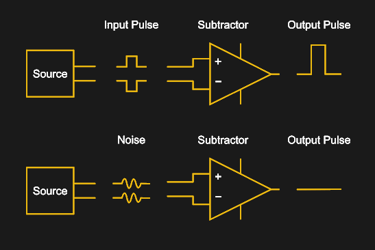
Differential signaling is commonly used in many communication protocols, including RS-422, IEA-485, Ethernet (via twisted-pair wiring), DisplayPort, HDMI and USB, as well as on PCBs, where the connection between the Ethernet PHY and magnetics is implemented as differential pairs. Each side of the pair conducts the same signal, just with one side having the inverted signal. Both sides have the same impedance, and are affected similarly by (electromagnetic) noise in the environment. As a result, when the receiver flips the inverted signal back and merges the two signals, noise in the signal will become inverted on one side (negative amplitude) and thus cancel out the noise on the non-inverted side.
The move towards lower signal voltages (in the form of LVDS) in these protocols and the increasing clock speeds makes the use of differential pairs essential. Fortunately they are not extremely hard to implement on, say, a custom PCB design. The hard work of ensuring that the traces in a differential pair have the same length is made easier by common EDA tools (including KiCad, Autodesk Eagle, and Altium) that thatl provide functionality for making the routing of differential pairs a semi-automated affair.
Having It Both Ways: SerDes
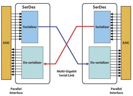
A Serializer/Deserializer (SerDes) is a functional block that is used to convert between serial data and parallel interfaces. Inside an FPGA or communications ASIC the data is usually transferred on a parallel interface, with the parallel data being passed into the SerDes block, where it is serialized for transmission or vice-versa. The PCIe PMA (physical media attachment) layer is the part of the protocol’s physical layer where SerDes in PCIe is located. The exact SerDes implementation differs per ASIC vendor, but their basic functionality is generally the same.
When it comes to producing your own PCIe hardware, an easy way to get started is to use an FPGA with SerDes blocks. One still needs to load the FPGA with a design that includes the actual PCIe data link and transaction layers, but these are often available for free, such as with Xilinx FPGAs.
PCIe HDL Cores
Recent Xilinx FPGAs not only integrate SerDes and PCIe end-point features, but Xilinx also provides free-as-in-beer PCIe IP blocks (limited to x8 at PCIe v2.1) for use with these hardware features that (based on the license) can be used commercially. If one wishes for a slightly less proprietary solution, there are Open Source PCIe cores available as well, such as this PCIe Mini project that was tested on a Spartan 6 FPGA on real hardware and provides a PCIe-to-Wishbone bridge, along with its successor project, which targets Kintex Ultrascale+ FPGAs.
On the other sides of the fence, the Intel (formerly Altera) IP page seems to strongly hint at giving their salesperson a call for a personalized quote. Similarly, Lattice has their sales people standing by to take your call for their amazing PCIe IP blocks. Here one can definitely see the issue with a protocol like PCIe: unlike ISA or PCI devices which could be cobbled together with a handful of 74xx logic chips and the occasional microcontroller or CPLD, PCIe requires fairly specialized hardware.
Even if one buys the physical hardware (e.g. FPGA), use of the SerDes hardware blocks with PCIe functionality may still require a purchase or continuous license (e.g. for the toolchain) depending on the chosen solution. At the moment it seems that Xilinx FPGAs are the ‘go-to’ solution here, but this may change in the future.
Also of note here is that the PCIe protocol itself is officially available to members of PCI-SIG. This complicates an already massive undertaking if one wanted to implement the gargantuan PCIe specification from scratch, and makes it even more admirable that there are Open Source HDL cores at all for PCIe.
Putting it Together
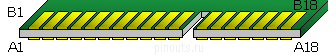
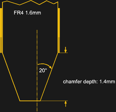
The basic board design for a PCIe PCB is highly reminiscent of that of PCI cards. Both use an edge connector with a similar layout. PCIe edge connectors are 1.6 mm thick, use a 1.0 mm pitch (compared to 1.27 mm for PCI), a 1.4 mm spacing between the contact fingers and the same 20° chamfer angle as PCI edge connectors. A connector has at least 36 pins, but can have 164 pins in an x16 slot configuration.
An important distinction with PCIe is that there is no fixed length of the edge connector, as with ISA, PCI and similar interfaces. Those have a length that’s defined by the width of the bus. In the case of PCIe, there is no bus, so instead we get the ‘core’ connector pin-out with a single lane (x1 connector). To this single lane additional ‘blocks’ can be added, each adding another lane that gets bonded so that the bandwidth of all connected lanes can be used by a single device.
In addition to regular PCIe cards, one can also pick from a range of different PCIe devices, such as Mini-PCIe. Whatever form factor one chooses, the basic circuitry does not change.
This raises the interesting question of what kind of speeds your PCIe device will require. On one hand more bandwidth is nice, on the other hand it also requires more SerDes channels, and not all PCIe slots allow for every card to be installed. While any card of any configuration (x1, x4, x8 or x16) will fit and work in an x16 slot (mechanical), smaller slots may not physically allow a larger card to fit. Some connectors have an ‘open-ended’ configuration, where you can fit for example an x16 card into an x1 slot if so inclined. Other connectors can be ‘modded’ to allow such larger cards to fit unless warranty is a concern.
The flexibility of PCIe means that the bandwidth scales along with the number of bonded lanes as well as the PCIe protocol version. This allows for graceful degradation, where if, say, a PCIe 3.0 card is inserted into a slot that is capable of only PCIe 1.0, the card will still be recognized and work. The available bandwidth will be severely reduced, which may be an issue for the card in question. The same is true with available PCIe lanes, bringing to mind the story of cryptocoin miners who split up x16 PCIe slots into 16 x1 slots, so that they could run an equal number of GPUs or specialized cryptocoin mining cards.
It’s Full of PCIe
This flexibility of PCIe has also led to PCIe lanes being routed out to strange and wonderful new places. Specifications like Intel’s Thunderbolt (now USB 4) include room for multiple lanes of PCIe 3.0, which enables fast external storage solutions as well as external video cards that work as well as internal ones.
Solid-state storage has moved over from the SATA protocol to NVMe, which essentially defines a storage device that is directly attached to the PCIe controller. This change has allowed NVMe storage devices to be installed or even directly integrated on the main logic board.
Clearly PCIe is the thing to look out for these days. We have even seen that System-on-Chips (SoCs), such as those found on Raspberry Pi 4 boards now come with a single PCIe lane that has already been hacked to expand those boards in ways thought inconceivable. As PCIe becomes more pervasive, this seems like a good time to become more acquainted with it.